<! this page under constructionThe SigDL SDK provides binary libraries, example C/C++ and Python source code, and demos for:
-
Deep learning model compression for IoT device and edge computing embedded systems
-
Deep learning model acceleration of training and testing in cloud and private servers
SigDL is aimed at IoT device and edge computing targets ranging in power consumption from wearables and mobile devices (1 to 3 W) to small form-factor servers (5 to 75 W). Functionality includes:
-
Support for deep learning models AlexNet, VGG-16, LeNet-5 and LeNet-300, and compressed models MobileNet and SqueezeNet
-
CICD continuous / iterative flow loop for cloud training and testing, compression, and embedded target training and testing, new data acquisition by the target
-
Support for embedded targets Nvidia Jetson TX2 (Parker SoC, Pascal GPU), Atom x5-E3930 and x5-E3940, multicore ARM, and Movidius MA2450
Deep Learning Model Compression
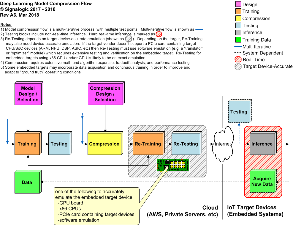
Model Compression Flow Diagram
Deep Learning Model Acceleration
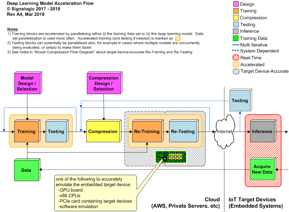
Model Acceleration Flow Diagram
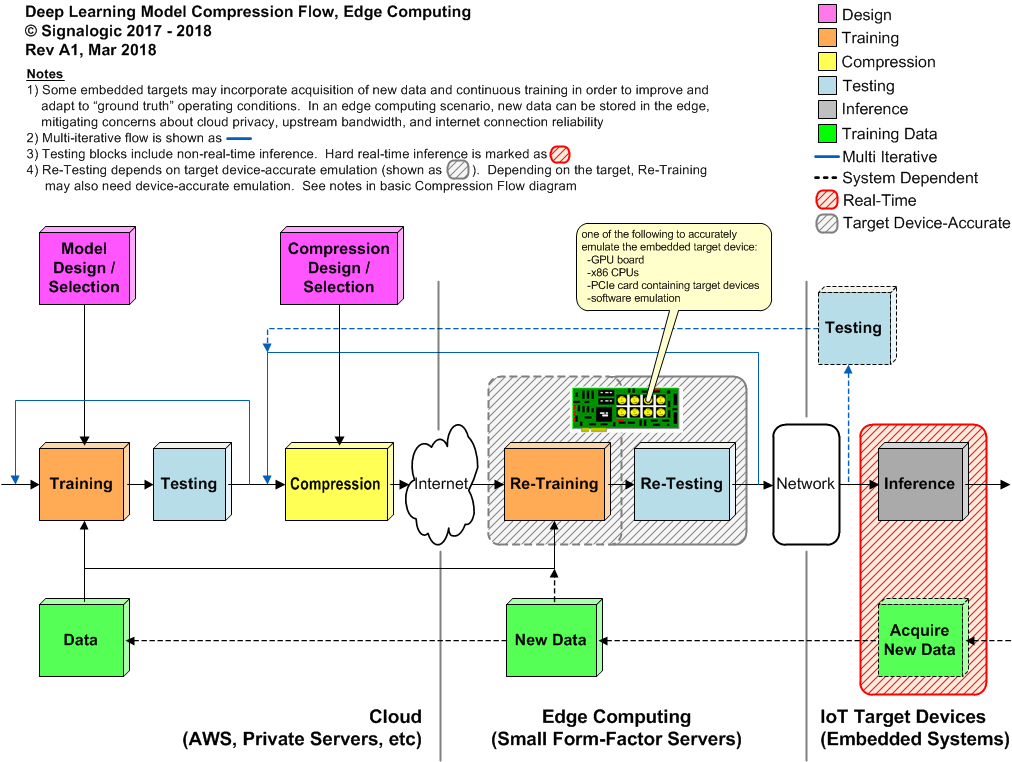
Deep Learning Edge Computing
Deep Learning Embedded Targets
Nvidia Jetson TX2
Intel Atom
Amazon DeepLens
Commercial pico-ITX and mini-ITX
Movidius (Intel) MA2450 Neural Net Chip
Texas Instruments c66x (pending, see notes)
Customized Deep Learning Embedded Targets
Model compression is the process of compressing and optimizing a deep learning model trained and tested in the cloud into a model suitable for real-time inference on an IoT or edge application embedded target. When tested on the embedded target with the identical data set used in cloud training, the model must perform with acceptable accuracy, real-time performance (for example, frames per sec), and meet application-defined power consumption requirements. Compression methods include basic approaches such as pruning, weight quantization and sharing, and weight encoding (for example Huffman coding), and more advanced approaches such as math algorithms that converts convolution layers to sparse matrices (under specific conditions) suitable for FFT processing; i.e. convolution in the frequency domain. Optimization methods include intrinsics, pragmas, loop reduction, and other target device specific techniques that apply to the compressed model. One example would be intrinsics that allow increased number of fixed-point operations per clock cycle, another would be a pragma that allows loop unrolling.
After compression and optimization methods are selected, the model must be retrained and retested using the compressed model in order to reach (i) a tolerable loss in accuracy (typically 2 - 5%) and (ii) required real-time performance (typically some number of frames per sec). Re-training and re-testing apply all changes resulting from compression and optimization, such as fixed-point weight values, weight sharing, data re-use, alternative math, and other algorithm changes. The overall process -- training, testing, compressing, retraining, and retesting -- may require many iterations until acceptable tradeoffs are reached. This is a time-consuming, iterative process that must be done on high performance cloud or private servers and not on the embedded target, where it would take prohibitive amounts of time.
Below is a flow diagram showing the multi-iterative, multi-testpoint nature of model compression. The objective is to map continuous integration and continuous deployment (CICD) onto available server resources (i.e. public cloud and/or private servers) and embedded targets (i.e. IoT and edge products).
Notes about model compression CICD flow:
-
All testing blocks include inference. For inference testing performance may vary from non-real-time to accelerated many times faster than real-time, depending on available cloud resources. An inference block is shown explicitly when real-time performance is required.
-
Re-Testing depends on how well cloud based compression testing can emulate the target; i.e. whether Re-Testing is target "device-accurate". If the target vendor does not support PCIe cards containing the same target CPU/SoC devices (ARM, NPU, DSP, ASIC, etc) -- or software emulation is used (e.g. a "translater" or "optimizer" module of some type) -- then it's likely that testing on the embedded target itself will be needed to verify model real-time performance and accuracy. In all cases, power consumption must be measured on the embedded target.
If the embedded target contains an Nvidia SoC, then Nvidia GPU boards with the same CUDA and/or Tensor core type can be used for Re-Training and Re-Testing. If the embedded target uses x86 CPU cores, then x86 server CPUs can be used for Re-Training and Re-Testing (preferably the same generation of x86 chip architecture). In both cases, limits on number of cores, clock rate, available memory, etc. can be enforced during Re-Testing in order to give reliable predictions of real-time performance and accuracy on the embedded target.
If the embedded target contains an SoC or CPU type that doesn't have an equivalent PCIe card (e.g. Intel Movidius) -- or it does but for whatever reason the vendor doesn't incorporate the PCIe card in their deep learning software tools (e.g. Texas Instruments) -- then software emulation using a "translator" tool is required. Such cross-chip approaches to model compression, retraining, and retesting are likely to be problematic, for example the translator software may be closed source, may take excessive time to run (and not allow parallelization), may not precisely emulate the target, or in the worst case, may not be well supported by the vendor. -
Re-Training using device-accurate target emulation (PCIe card, software, etc as mentioned in note 2) is not required, but may produce a compressed model that reduces Re-Testing time, thus reducing overall CICD loop time.
-
Compression requires math and algorithm expertise and tradeoff analysis. Some concepts are basic such as quantization and weight sharing, others require advanced math, for example sparse matrix and FFT based computation.
-
It's expected that embedded targets will incorporate data acquisition for additional training and performance adaptation. This leads to the CICD requirement, as noted above.
In the following description, "acceleration" means as-fast-as-possible training performance in the cloud, using whatever cloud resources are available or can be procurred. Some deep learning researchers use "acceleration" to mean inference performance improvement; for embedded targets, this is incorrect usage as the question is simply whether the embedded target / product is running inference in real-time, and what level of optimization is required to achieve that. For example, for video or image based applications, does performance meet the fps (frames per sec) product requirement ? The answer is a function of model compression and other optimizations applied to the inference run-time. Maintaining a clear distinction in these terms allows a compressed and optimized model to also be accelerated, for example the Re-Testing block can be accelerated, or multiple compressed models can be tested / evaluated concurrently. To summarize, in the software and hardware descriptions on this page, "compression" and "optimization" mean achieving real-time inference (in the product), and "acceleration" means reducing time required for training and testing (in the cloud).
Below is a flow diagram showing deep learning model acceleration. Like model compression above, the process is multi-iterative with multiple test points. In this case, the focus is on accelerating model training, for example reducing training time to a day or several hours, or possibly less. When combined with model compression, the primary objectives are (i) map continuous integration and continuous deployment (CICD) onto available server resources (i.e. public cloud and/or private servers) and embedded targets (i.e. edge and IoT products), and (ii) minimize CICD redeployment time, in order to increase reliability and robustness of edge and IoT products.
Notes about the above flow diagram:
-
Training blocks are accelerated by parallelizing either (i) the training data set or (ii) the deep learning model. Data set parallelization is used more often. Tim Dettmer's Parallelize Deep Learning on GPUs page has a good explanation of the tradeoffs in these two approaches.
-
The initial Training block assumes use of GPU boards of some type.
-
Re-Testing depends on device-accurate emulation of the embedded target. It can also be accelerated, although it may depend on the emulation method; for example, the number of concurrent processes supported by the target device PCIe card (if one is being used). See compression flow diagram note 2) above for a more in-depth discussion of target emulation.
-
Re-Testing results must be evaluated for accuracy and performance. It may also be possible to make an approximate estimate of target power consumption, although reliable "real world" values can only be obtained by running real-time inference on the target.
-
Testing blocks can potentially be parallelized, for example in cases where multiple compression models are concurrently being evaluated, or to simply make them faster. In either case the data set can be divided into groups, and results aggregated upon completion.
There is an increasing need to push deep learning training, compression, and testing into edge computing, closer to IoT product targets, in order to mitigate latency, internet connection reliability, privacy, and upstream bandwidth cloud weaknesses. In a CICD solution, upstream bandwidth is of particular concern when IoT products continuously acquire new data for re-training and re-testing. Some product examples include:
-
a local network of ultra low power smart cameras, with local servers providing re-training and re-testing to generate updated real-time inferences, allowing any one camera to update knowledge shared among cameras
-
driverless vehicles where acquired new data must be stored temporarily in on-vehicle servers for processing to remove private information (people on private property, license plates, etc)
-
medical applications where bandwidth and privacy limitations prevent use of remote cloud / data centers, and on-premise servers must be small, quiet, and very low power
Below is a flow diagram showing edge computing model compression re-training and re-testing. Note that cloud data can be updated also, as latency and upstream bandwidth permits. Any data considered private can remain in edge storage.
Work is ongoing to support the following embedded targets with SigDL software. The following sections take a closer look at available deep learning product platforms and form-factors that range in power consumption from 1 to 75 W.
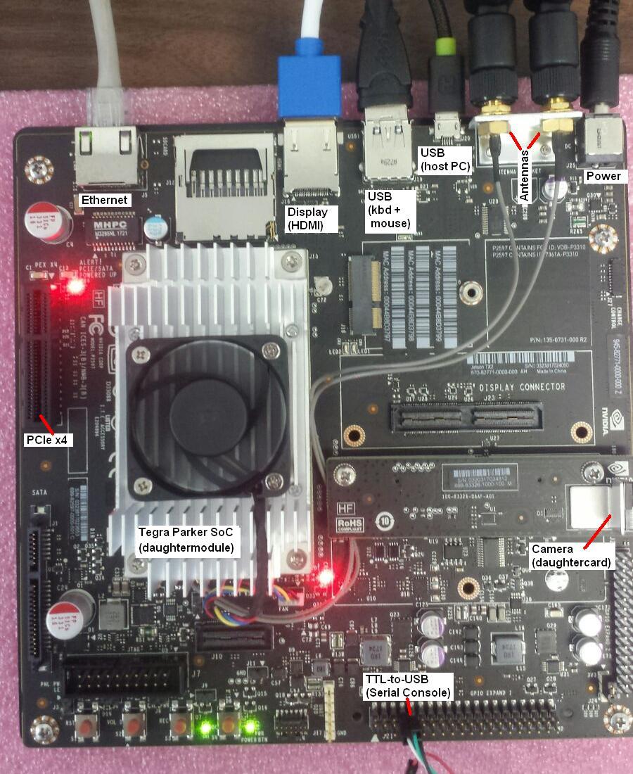
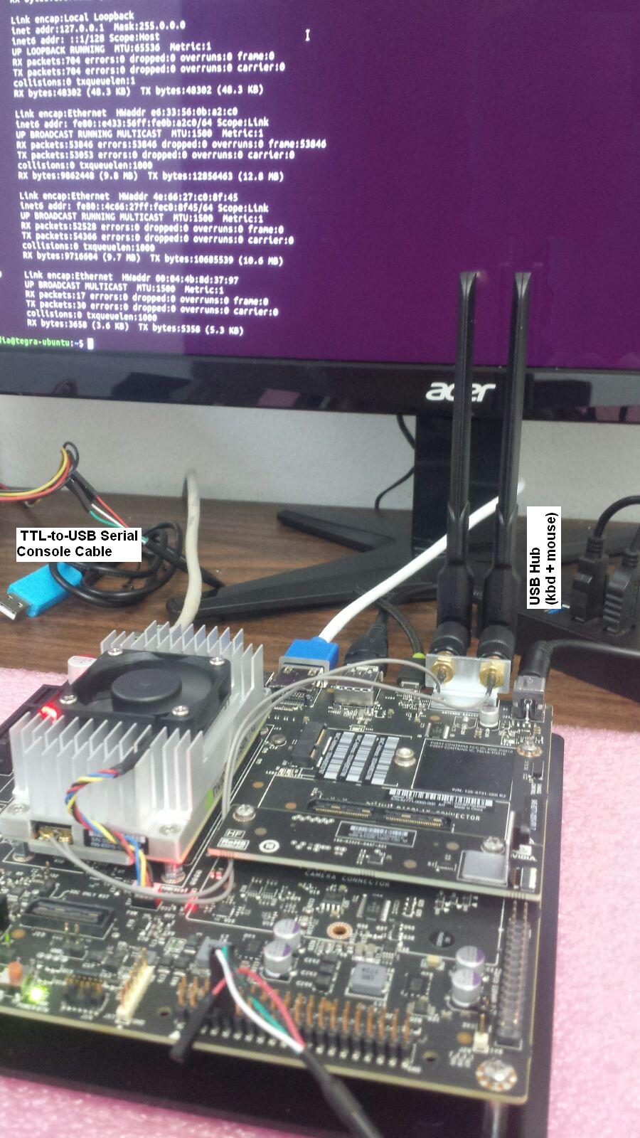
The Jetson TX2 is a development board containing a Tegra family "Parker" SoC with 256 Cuda GPU cores. Below is an image showing the Jetson TX2 board set up in the lab, with key TX2 peripherals labeled. Note the small camera daughtercard at right.
If used as-is in an embedded product, the Jetson TX2 consumes from 7 to 15 W, which is at the high end of power consumption for IoT device applications, and low end for edge computing applications. Custom IoT device applications incorporating the Parker SoC may reduce power consumption by carefully controlling clock rate and peripheral usage. Note that the Parker SoC always requires a heat sink; depending on Cuda core usage, a fan may or may not be needed.
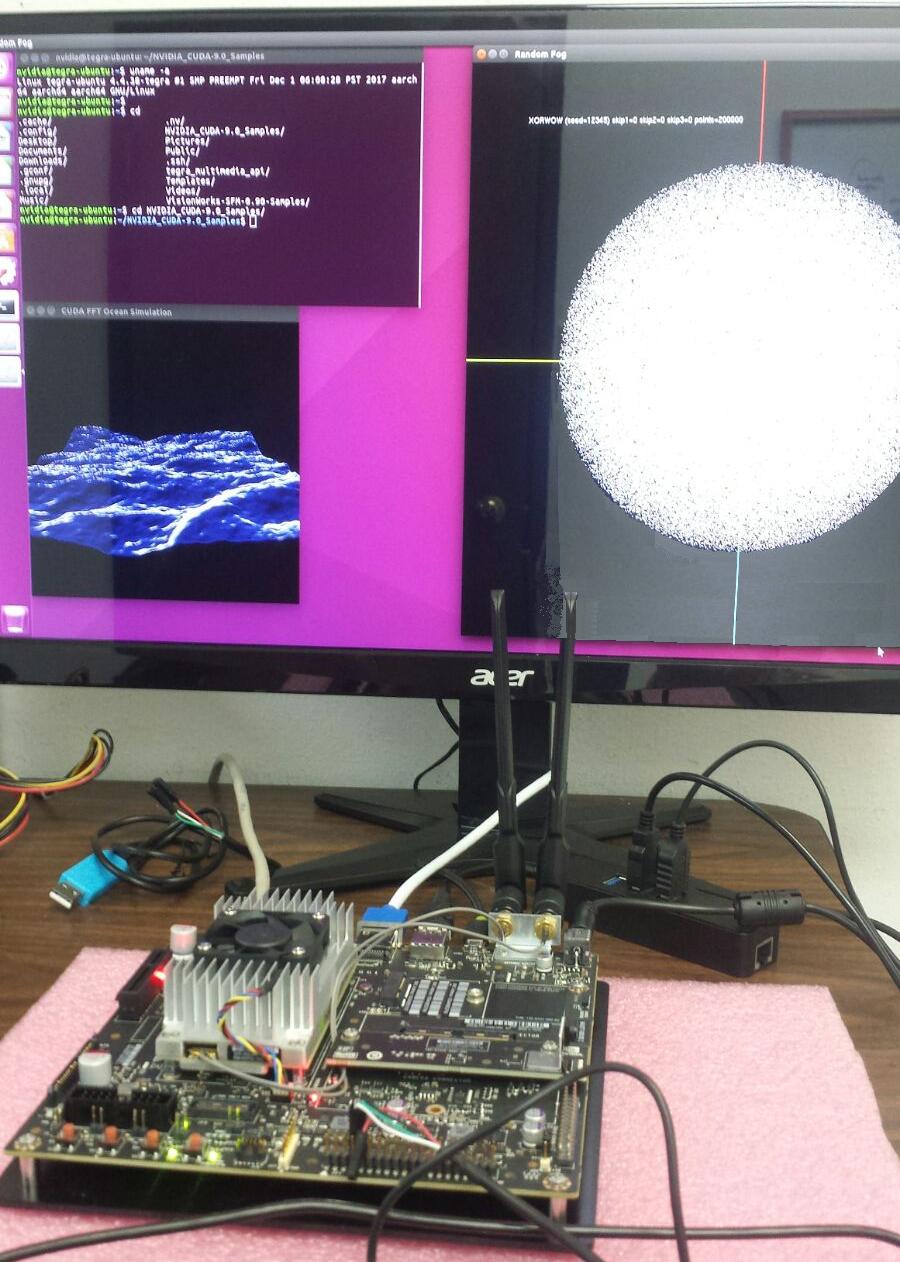
Below is an image showing an expanded view of the Jetson TX2 board set up in the lab. Note the requirement for a USB hub to use the integrated keyboard and mouse, and also the "TTL to USB" cable required for a serial debug console.
Below the "ocean FFT" and "random fog" CUDA demos are running. For deep learning, inference run-times can be downloaded and run via remote log-in, which is a requirement for CIDC cloud based model compression, as described above.
The deep learning embedded targets below use Atom x5-E39xx family CPUs, but vary in SWaP 1, making them suitable for IoT and edge products with power consumption ranging from 7 to 15 W. Using an x86 compatible CPU offers advantages in (i) compatibility with a wide variety of software, (ii) fast development time, and (iii) support for a huge range of I/O and storage peripherals.
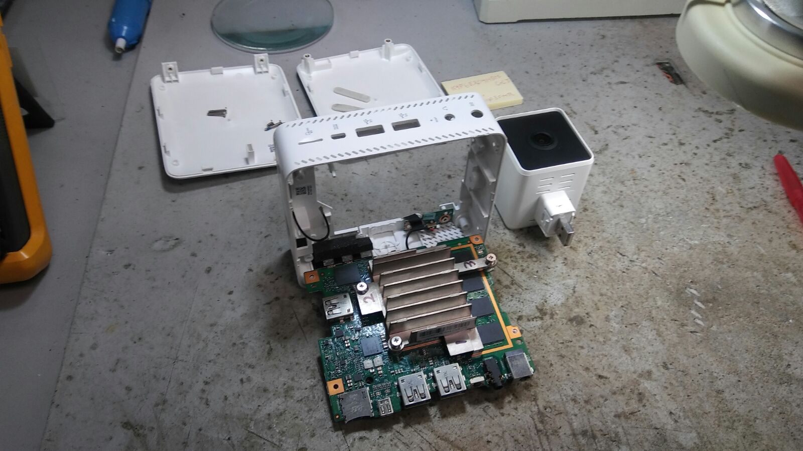
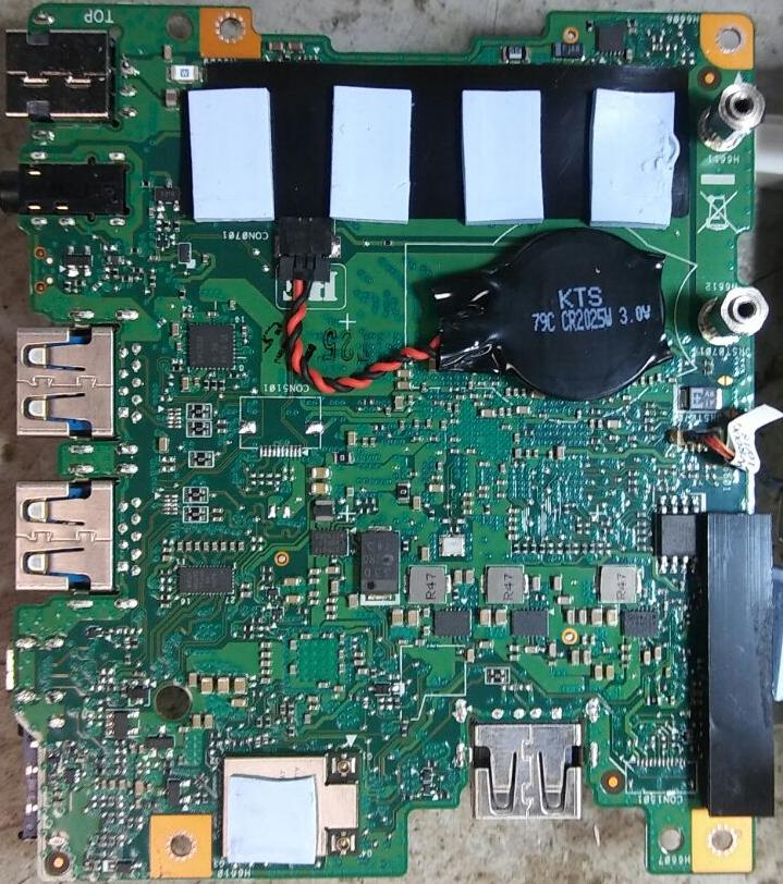
In terms of SWaP, Amazon AWS's DeepLens represents the current state-of-the-art lower boundary for x86 CPU based deep learning IoT and edge products. In a way, Amazon is competing for the "smallest possible x86 server"; the images below provide some insight into the challenges they faced. The first image is a partial disassembly view. Note the small form-factor motherboard, incorporating mobile phone PCB technology (such as ultra fine-pitch connectors and FBGA packages, blind and buried vias and microvias, and extensive use of 0201 and 1005 discrete component package sizes). An Atom x5-E3930 dual-core CPU (1.3 GHz, 6.5 W TDP) is under the heat sink (there are no fans in the enclosure).
Also note the use of a USB camera interface. For applications requiring multiple cameras, or a multichannel combination of vision and audio I/O, adding more USB ports is straightforward when running Linux on an x86 CPU.
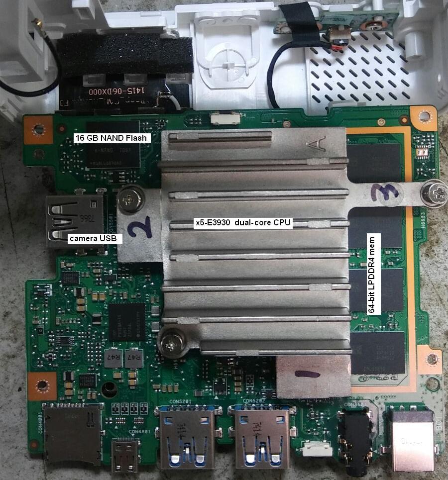
Below is a top (component) side view of the DeepLens motherboard:
In any deep learning IoT product design, minimizing memory power consumption is crucial, but it's especially important for x86 CPU based designs, which require sizable external memory capacity in order to gain maximum advantage from running Linux and open source software (much of which is developed and runs in the cloud). The DeepLens uses LPDDR4 DRAM, often referred to as "mobile DRAM" (i.e. cell phone memory technology). The DeepLens has 8 GB of DRAM memory, implemented as four (4) Samsung 16 Gb x16 external devices (64-bit wide interface, maximum of 3733 Mbps transfer rate from a 233 MHz clock). Non-volatile storage is provided by an SK Hynix 16 GB NAND Flash chip.
Although the fanless DeepLens enclosure provides a great example of what's currently possible with x86 CPUs inside IoT and edge products, Intel still has a ways to go to improve the situation. The x5 CPU family generates enough heat that external LPDDR4 devices must be placed a considerable distance from the CPU (due to the mechanical size of the heat sink), which impacts both memory performance and overall size of the motherboard. A desirable objective for future x86 CPU chip designs would be to use PoP (package on package) technology to allow memory devices to "stack" directly on top of the CPU. However, this will take another major reduction in CPU power consumption.
Below is a bottom (solder) side view of the DeepLens motherboard:
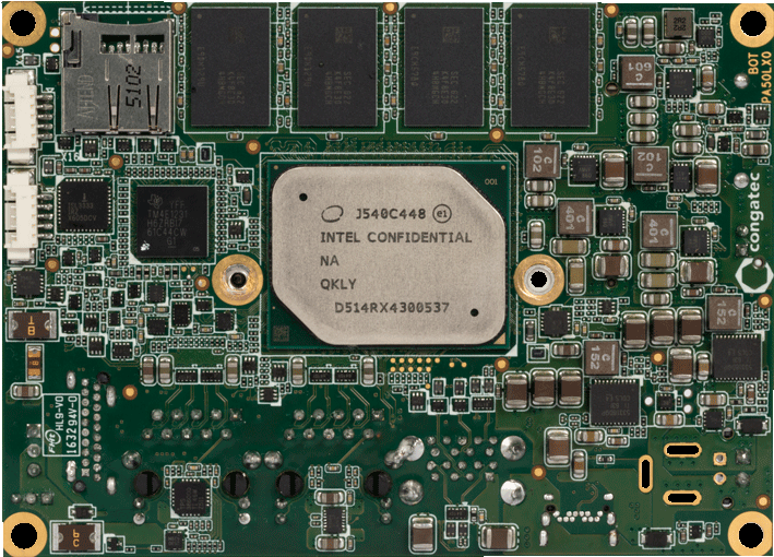
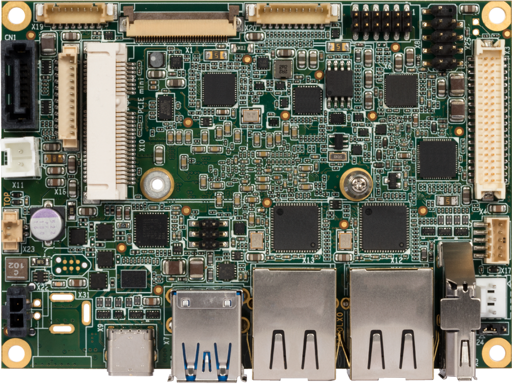
Below is an image of a commercially available pico-ITX form-factor board 2, with an Atom x5-E3930 dual-core CPU (same as the DeepLens). Note the PCB dimensions (100 x 70 mm per pico-ITX standard) are slightly smaller than the DeepLens PCB (100 x 87 mm).
Although the Atom CPU is visible in the above image, it needs a heat sink for normal operation. Below is an image of the pico-ITX motherboard component side, including all connectors:
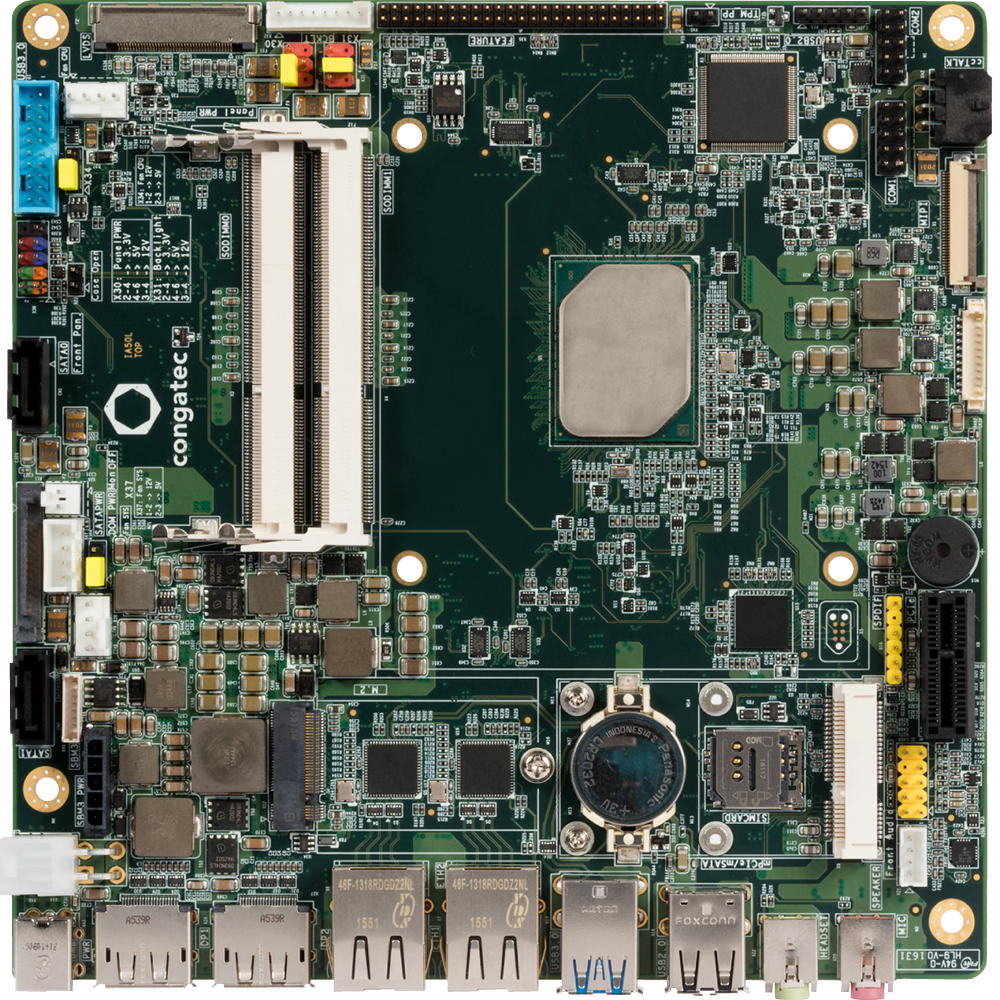
Below is an image of a commercially available mini-ITX form-factor board 2, with an Atom x5-E3940 quad-core CPU. Compared to the DeepLens CPU, the x5-E3940 has 2 additional cores, runs at 1.6 GHz and has a higher power rating (9.5 W vs. 6.5 W TDP).
1 SWaP = size, weight, and power consumption.
2 The commercial pico-ITX and mini-ITX board images are web pics of Congatech PA5 and IA5 products; we don't have these in our lab yet.
The Movidius neural net devices are small, very low power ASICs intended for use in IoT device products. The example shown here is a Myriad 2 MA2450 chip that highly optimizes a compressed deep learning model in order to minimize the chip's SWaP.
Using ASICs, a compressed deep learning model can run under 1 W. Of course there are tradeoffs in this approach; namely the system still needs another device (say an ARM) to run Linux, other general software, and likely some amount of OpenCV image processing, which consumes a substantial amount of additional power. Another less obvious tradeoff is that typically only one compressed model (in the case of the Movidius device, MobileNet) is supported, and flexibility in model parameters, such as input image resolution and convolutional layer resolution, is limited.
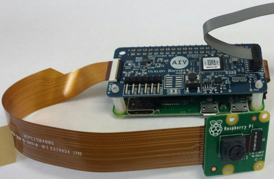
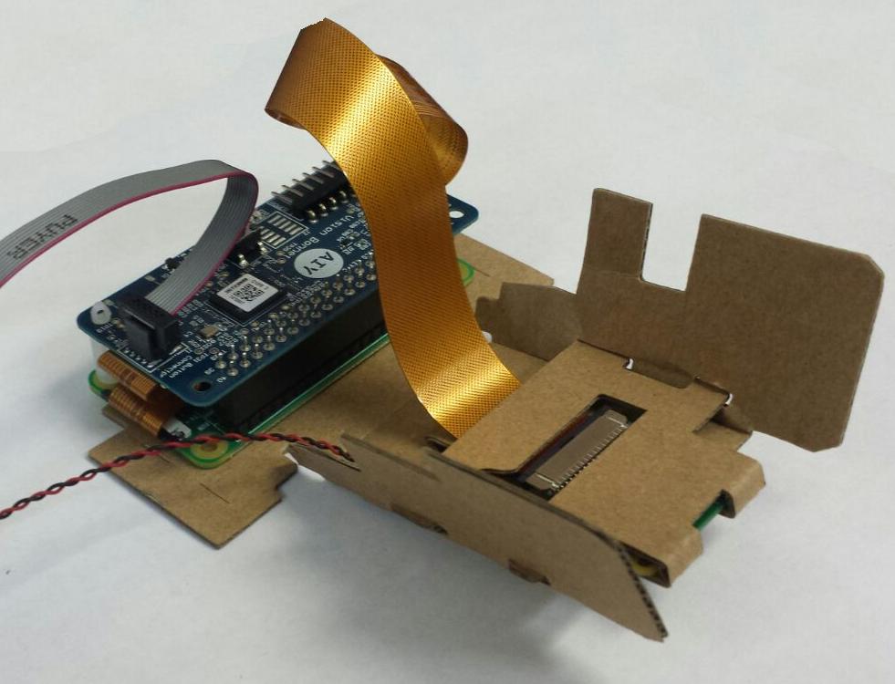
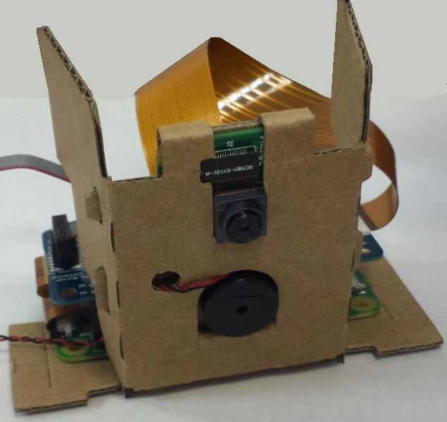
Below are some lab pics showing internal assembly and cabling of the AIY vision kit, which incorporates the Movidius device. The assembly is formed by attaching a daughtermodule containing the Movidius device and a v2 camera module to a Raspberry Pi Zero W. The Zero W version of Raspberry Pi modules is required as it has a fine pitch FPC (Flexible Printed Circuit) connector for the camera.
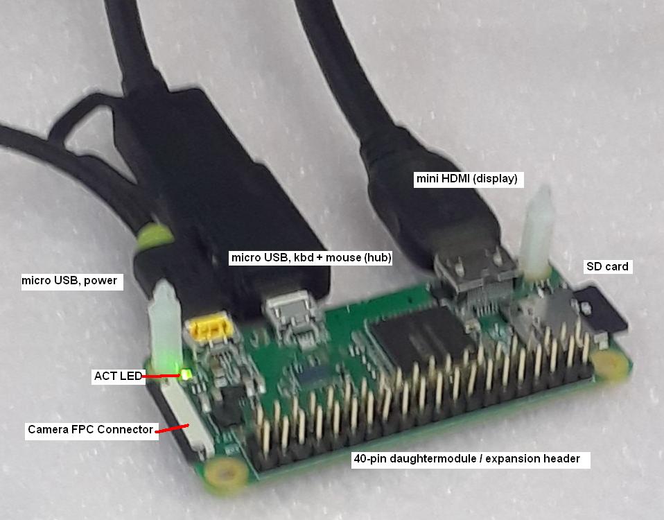
The image below shows the Raspberry Pi Zero W module by itself, without the Movidius daughtermodule attached. The 40-pin header is used by the Raspberry Pi community for expansion purposes by attaching a wide variety of daughtermodules. Note the camera connector at left, and also the ACT (activity LED) near the micro USB power connector, which is used to indicate boot activity.
Looking closely at the Raspberry Pi Zero W, you might ask, where is the memory ? How can the PCB be so small ? The answer is the Raspberry Pi module series are highly advanced, state-of-the-art examples of embedded system engineering. Most impressive is the small size of the Zero W PCB, which eliminates all FBGA packages except a Broadcom ARM SoC, and uses PoP technology (package on package) to stack memory directly on top of the SoC.
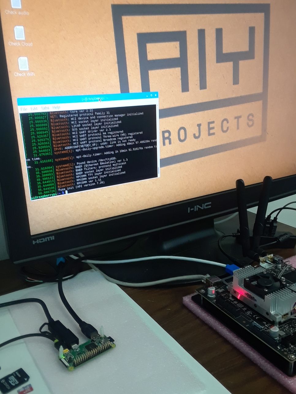
The image below shows dmesg after a Raspberry Pi Zero W boot, still without the Movidius vision module or camera attached. Note that the Raspberry Pi SoC contains a simple onchip boot loader which does a few SoC initialization steps, but from that point forward is entirely dependent on micro SD card contents (the boot process is documented on this stackexchange thread).
The next set of images show the Raspberry Pi Zero W module with the Movidius vision daughtermodule attached, and the camera connected, from different perspectives.
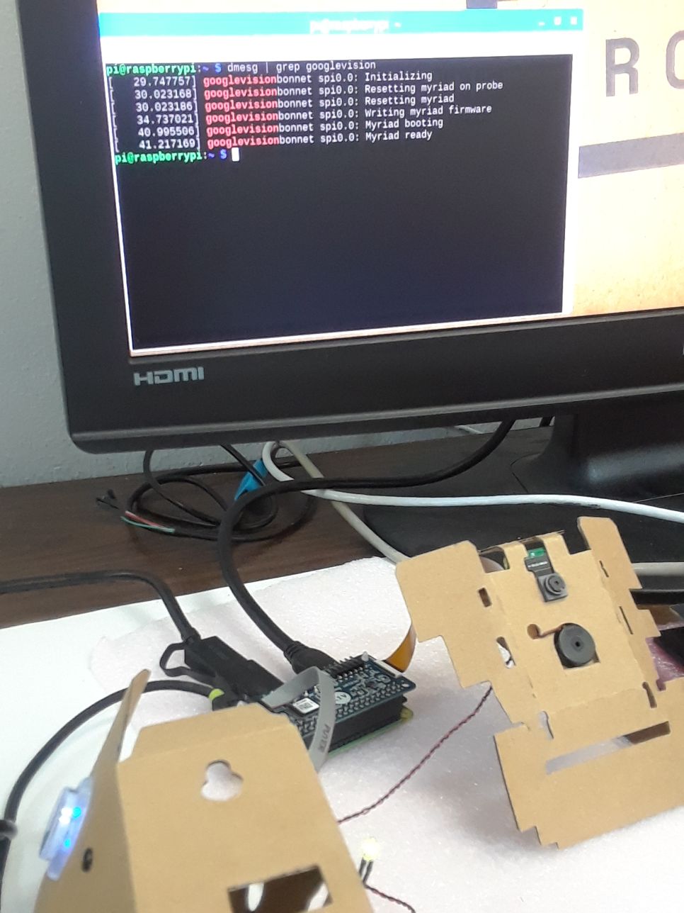
The image below shows dmesg display, grepped for "googlevision", after booting with the Movidius vision module and camera attached. A couple of notes about AIY nomenclature:
-as noted above, the Movidius ASIC chip is also known as "Myriad"
-"Bonnet" is a Googly word for daughtermodule
Terms like AIY and Bonnet sound friendly, and the Raspberry Pi does run Linux, but make no mistake: solving debug and development problems at this level of miniaturization is not easy. Gritty methods such as hand-soldering under a microscope and lab equipment such as JTAG emulator, digital scope, and logic analyzer, may be needed. Fortunately, embedded system development and debug has a long history of established methods and techniques, stretching back to PC104 technology in the 1990s.
Fundamentally, TI devices containing c66x cores are able to perform energy-efficient, high performance deep learning, as demonstrated in this deep learning embedded target comparison paper by Dr. Nachiket Kapre at the University of Waterloo. It's unknown if TI will embrace the need for a cloud based deep learning solution that supports c66x device-accurate CICD flow, including model compression, re-training, and re-testing. The current TIDL (TI Deep Learning) solution, which supports ADAS and other embedded devices containing c66x cores, uses software emulation (see "Notes about model compression CICD flow", above).
As a potential basis for a c66x device-accurate cloud solution, the architecture shown in the pictures and links already works for HPC applications and can be adapted. Currently this architecture supports OpenCV, C/C++, Python, c66x math and DSP libraries, 8-bit MAC operations (32-bit accumulation), and other essential deep learning components, but a substantial amount of additional work is needed to create a deep learning CICD reference solution. At minimum, such a solution should incorporate TensorFlow, Caffe, and the deep learning and compression models mentioned in the Readme intro above.
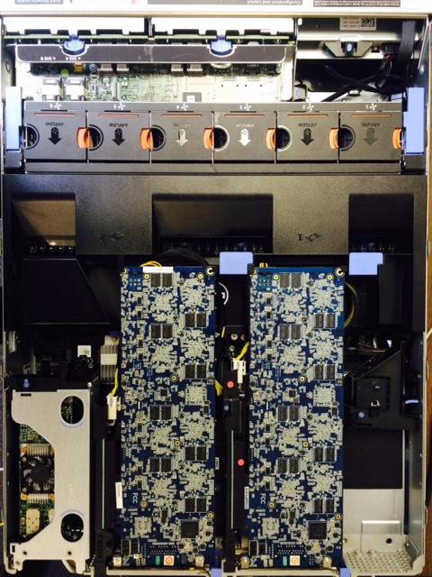
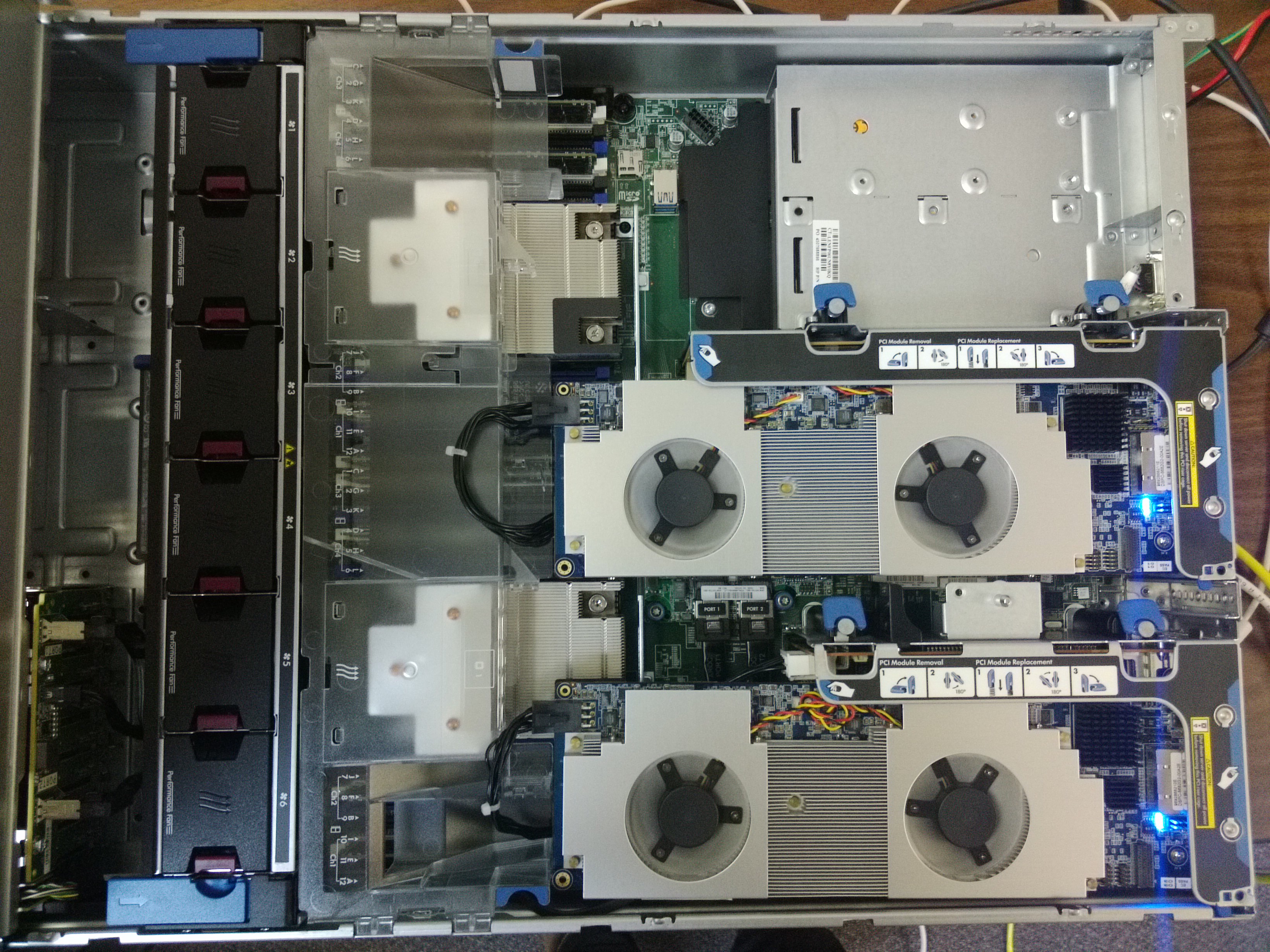
The images below show multiple 64-core PCIe cards (up to 384 or more c66x cores depending on server form-factor, suitable for training on high resolution data sets), in standard 1U and 2U Dell and HP servers.
For detailed information on the underlying technology of combined c66x + x86 architecture solutions, see the TI wiki pages for HPC, c66x OpenCV, and NFV Transcoding.
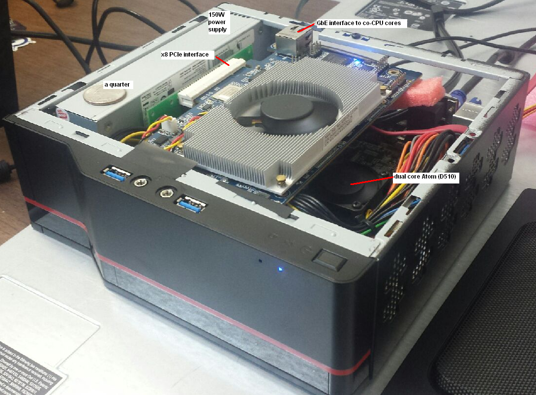
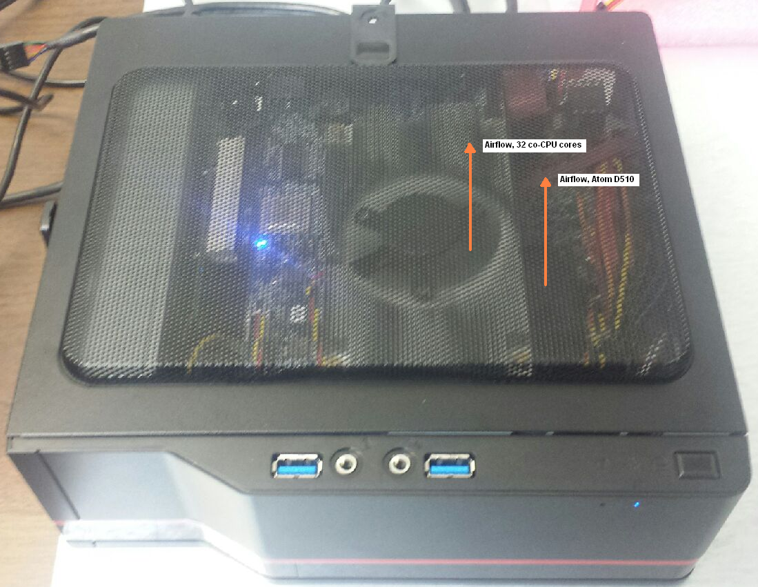
In addition to the above "pure cloud" solutions, the combined c66x + x86 architecture can also target small-form factor edge computing servers in the 30 to 70 W range. The images below show a combination of Atom x86 and TI c66x cores in a mini-ITX format, with 32 to 64 c66x cores accessible as half-size PCIe card(s).
In the mini-ITX images, the motherboard is a dual core Atom (C2358 @ 1.74 GHz) with 4x GbE interfaces, and 8 GB DDR3 mem @ 1333 MHz. A more suitable motherboard would contain x5-E39xx dual-core or quad-core Atom, with either a x4 or x8 PCIe slot (or mPCIe interface).
As an interesting side note, besides x86 it's also possible to combine a half-size c66x PCIe card Tegra GPU SoCs, for example the Jetson TX2 board has an x4 PCIe slot (see Jetson pics above). What are the possibilities in edge computing applicaitions of a mini-ITX server containing next-gen Tegra (say 128 CUDA cores and 128 Tensor cores) and 32 c66x cores ?
If you are using or considering to use TI c66x and wish to discuss this either with Signalogic or 3-way with TI Sr. Management, please contact Signalogic.
For information about customizing the above deep learning embedded targets, or developing something different based on combinations of the above targets or a new target, send e-mail to info at signalogic dot com.
